The ALS mission is to advance science for the benefit of society by providing our world-class synchrotron light source capabilities and expertise to a broad scientific community.
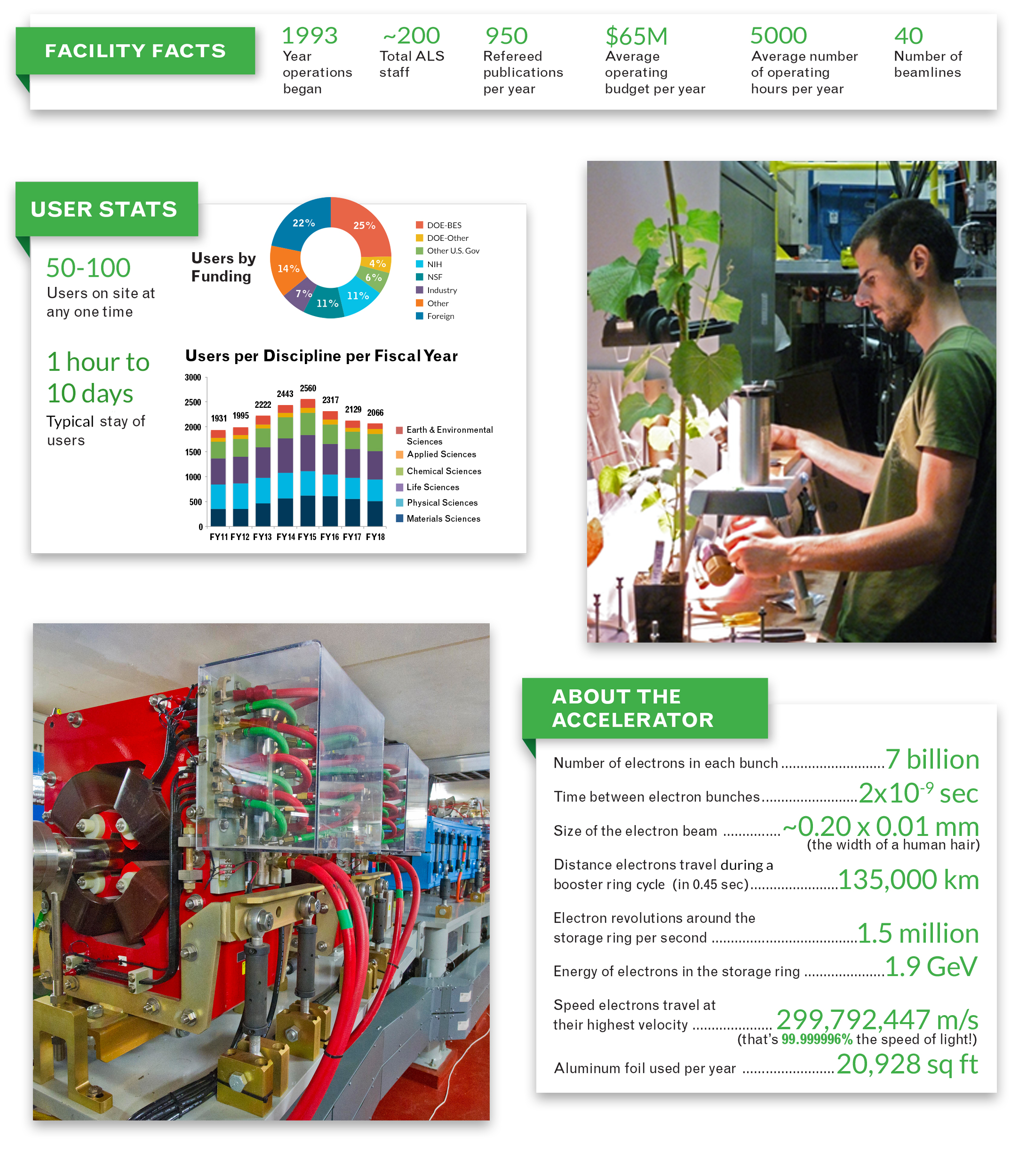
Quick Facts
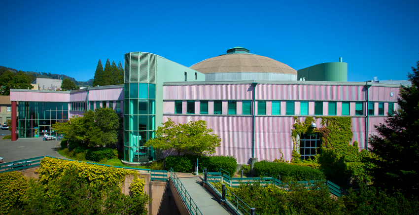
The Advanced Light Source (ALS) is a specialized particle accelerator that generates bright beams of x-ray light for scientific research. Electron bunches travel at nearly the speed of light in a circular path, emitting ultraviolet and x-ray light in the process. The light is directed through about 40 beamlines to numerous experimental endstations, where scientists from around the world (“users”) can conduct research in a wide variety of fields, including materials science, biology, chemistry, physics, and the environmental sciences. Operation of the ALS is funded by the U.S. Department of Energy, Office of Science, Basic Energy Sciences program.
The wavelengths of the synchrotron light span the electromagnetic spectrum from infrared to x-rays and have just the right size and energy range for examining the atomic and electronic structure of matter. These two kinds of structure determine nearly all the commonly observed properties of matter, such as strength, chemical reactivity, thermal and electrical conductivity, and magnetism. The ability to probe these structures allows us to design materials with particular properties and understand biological processes inscrutable to visible light.