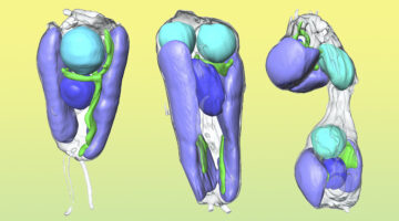
Researchers found that a symbiont capable of fixing nitrogen (turning it into a biologically usable form) has evolved into an organelle—an intrinsic part of the algae cells that host it. The discovery is of great interest for understanding organelle genesis and for efforts to engineer agricultural plants with built-in nitrogen-fixing capabilities. Read more »![]()
All News & Updates
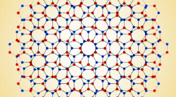
Scientists Discover First Nitrogen-Fixing Organelle
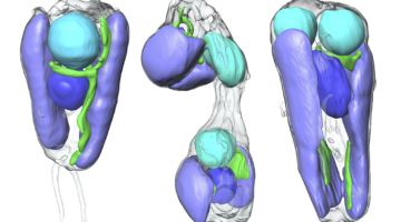
In two recent papers, an international team of scientists describe the first known nitrogen-fixing organelle within a eukaryotic cell. The organelle is the fourth example in history of primary endosymbiosis—the process by which a prokaryotic cell is engulfed by a eukaryotic cell and evolves beyond symbiosis into an organelle. Read more »
Shedding Light on Sea Creatures’ Secrets
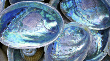
Exactly how does coral make its skeleton, a sea urchin grow a spine, or an abalone form the mother-of-pearl in its shell? A new study at the ALS revealed that this process of biomineralization, which sea creatures use to lock carbon away in their bodies, is more complex and diverse than previously thought. Read more »
Suggest Speakers and Workshops for the 2024 User Meeting

The 2024 ALS User Meeting will take place August 12–14. Help shape this year’s program by submitting nominations for plenary speakers and proposing workshops and tutorials by April 4. Read more »
Winter 2024 Shutdown Recap
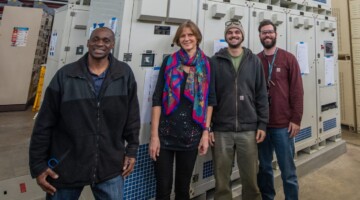
The ALS is back in user operation after more than two months of shutdown. Major achievements include the mechanical installation for the new booster bend power supplies and the two power supplies for the accumulator ring radio frequency system. Read more »
Room-Temperature 2D Magnet: Electronic-Structure Insights
Researchers found that small changes in how electron spins interact with each other can make a big difference in the magnetic transition temperatures of 2D magnets. Understanding such factors can help create better magnetic materials for information storage, sensors, medical imaging, and energy-efficient computing. Read more »![]()
![]()
Monika Choudhary, Computing Postdoc
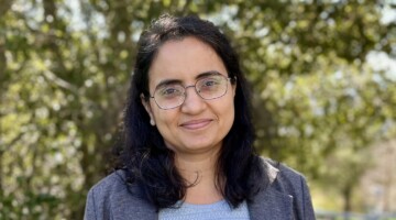
As a postdoc, Monika Choudhary applies computing models to real experimental data at the ALS, work that uses her extensive computer science knowledge and experience. Read more about the path that led her to the ALS and the people she’s met along the way. Read more »
Clarifying the FLASH Effect for Cancer Radiation Therapy
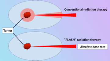
To clarify the underlying mechanisms of the FLASH effect, in which the delivery of ultrafast, high-intensity doses of radiation to tumors counterintuitively reduces damage to surrounding healthy cells, researchers directly compared the oxidative effects of conventional and FLASH techniques using x-ray footprinting at the ALS. Read more »
Case Study of Aerosol Particles Influenced by Wildfire
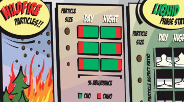
Researchers studied atmospheric aerosols influenced by wildfires in the Pacific Northwest. They examined the connection between particle size, chemical composition, and phase state, in particles collected during the day and at night. The information is important for modeling the effects of wildfire smoke on atmospheric properties. Read more »
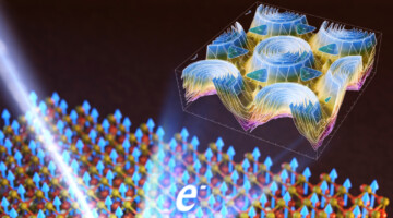
Big Twist Leads to Tunable Energy Gaps in a Bilayer Stack
Researchers found that twisting 2D layers at atypically large angles opens up potentially useful energy gaps in the material’s band structure. The results suggest a new way to tune materials for optoelectronic applications and provides a platform for exploring novel “moiré” phenomena beyond those observed at small twist angles. Read more »![]()
![]()
- 1
- 2
- 3
- …
- 123
- Next Page »